
Page 75 - Kingbright 2022-2023 catalog
P. 75
TECHNICAL NOTES
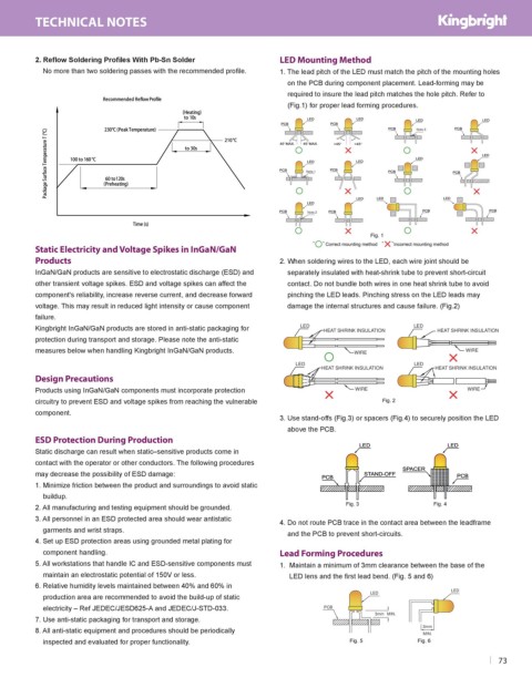
2. Reflow Soldering Profiles With Pb-Sn Solder LED Mounting Method
No more than two soldering passes with the recommended profile. 1. The lead pitch of the LED must match the pitch of the mounting holes
on the PCB during component placement. Lead-forming may be
required to insure the lead pitch matches the hole pitch. Refer to
(Fig.1) for proper lead forming procedures.
Note.3
. .
Note.1
Note.2
Fig. 1
Static Electricity and Voltage Spikes in InGaN/GaN
Products 2. When soldering wires to the LED, each wire joint should be
InGaN/GaN products are sensitive to electrostatic discharge (ESD) and separately insulated with heat-shrink tube to prevent short-circuit
other transient voltage spikes. ESD and voltage spikes can affect the contact. Do not bundle both wires in one heat shrink tube to avoid
component's reliability, increase reverse current, and decrease forward pinching the LED leads. Pinching stress on the LED leads may
voltage. This may result in reduced light intensity or cause component damage the internal structures and cause failure. (Fig.2)
failure.
Kingbright InGaN/GaN products are stored in anti-static packaging for LED HEAT SHRINK INSULATION LED HEAT SHRINK INSULATION
protection during transport and storage. Please note the anti-static
measures below when handling Kingbright InGaN/GaN products. WIRE WIRE
LED LED
HEAT SHRINK INSULATION HEAT SHRINK INSULATION
Design Precautions
Products using InGaN/GaN components must incorporate protection WIRE WIRE
circuitry to prevent ESD and voltage spikes from reaching the vulnerable Fig. 2
Fig. 2
component.
3. Use stand-offs (Fig.3) or spacers (Fig.4) to securely position the LED
above the PCB.
ESD Protection During Production
Static discharge can result when static–sensitive products come in
contact with the operator or other conductors. The following procedures
may decrease the possibility of ESD damage:
1. Minimize friction between the product and surroundings to avoid static
buildup.
2. All manufacturing and testing equipment should be grounded. Fig. 3 Fig. 4
3. All personnel in an ESD protected area should wear antistatic 4. Do not route PCB trace in the contact area between the leadframe
garments and wrist straps. and the PCB to prevent short-circuits.
4. Set up ESD protection areas using grounded metal plating for
component handling. Lead Forming Procedures
5. All workstations that handle IC and ESD-sensitive components must 1. Maintain a minimum of 3mm clearance between the base of the
maintain an electrostatic potential of 150V or less. LED lens and the first lead bend. (Fig. 5 and 6)
6. Relative humidity levels maintained between 40% and 60% in LED
production area are recommended to avoid the build-up of static LED
electricity – Ref JEDEC/JESD625-A and JEDEC/J-STD-033. PCB
3mm MIN.
7. Use anti-static packaging for transport and storage.
3mm
8. All anti-static equipment and procedures should be periodically
MIN.
Fig. 6
Fig. 5
inspected and evaluated for proper functionality. Fig. 5 Fig. 6
73