
Page 76 - Kingbright 2022-2023 catalog
P. 76
TECHNICAL NOTES
2. Lead forming or bending must be performed before soldering, never Cleaning
during or after soldering. For SMD and through-hole LEDs
3. Do not stress the LED lens during lead-forming in order to prevent 1. Isopropyl alcohol or deionized water are recommended for cleaning.
fractures in the epoxy lens and damage the internal structures. Do not use acidic solvents or unknown chemicals, as they might cause
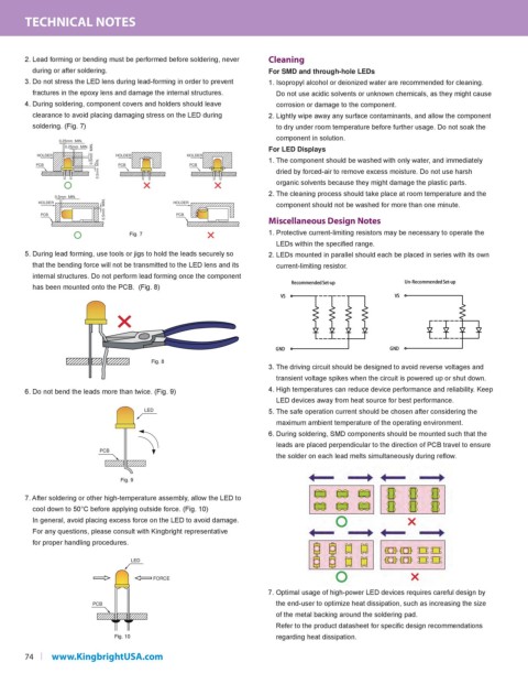
4. During soldering, component covers and holders should leave corrosion or damage to the component.
clearance to avoid placing damaging stress on the LED during 2. Lightly wipe away any surface contaminants, and allow the component
soldering. (Fig. 7) to dry under room temperature before further usage. Do not soak the
component in solution.
0.25mm MIN.
0.25mm MIN. For LED Displays
HOLDER 0.5mm MIN. HOLDER HOLDER 1. The component should be washed with only water, and immediately
0.5mm MIN. dried by forced-air to remove excess moisture. Do not use harsh
PCB PCB PCB
organic solvents because they might damage the plastic parts.
2. The cleaning process should take place at room temperature and the
0.5mm MIN.
0.5mm MIN.
HOLDER HOLDER component should not be washed for more than one minute.
PCB PCB Miscellaneous Design Notes
Fig. 7 1. Protective current-limiting resistors may be necessary to operate the
Fig. 7
LEDs within the specified range.
5. During lead forming, use tools or jigs to hold the leads securely so 2. LEDs mounted in parallel should each be placed in series with its own
that the bending force will not be transmitted to the LED lens and its current-limiting resistor.
internal structures. Do not perform lead forming once the component
has been mounted onto the PCB. (Fig. 8)
Fig. 8
3. The driving circuit should be designed to avoid reverse voltages and
transient voltage spikes when the circuit is powered up or shut down.
6. Do not bend the leads more than twice. (Fig. 9) 4. High temperatures can reduce device performance and reliability. Keep
LED devices away from heat source for best performance.
LED 5. The safe operation current should be chosen after considering the
maximum ambient temperature of the operating environment.
6. During soldering, SMD components should be mounted such that the
leads are placed perpendicular to the direction of PCB travel to ensure
PCB
the solder on each lead melts simultaneously during reflow.
Fig. 9
Fig. 9
7. After soldering or other high-temperature assembly, allow the LED to
cool down to 50°C before applying outside force. (Fig. 10)
In general, avoid placing excess force on the LED to avoid damage.
For any questions, please consult with Kingbright representative
for proper handling procedures.
LED
FORCE
7. Optimal usage of high-power LED devices requires careful design by
PCB the end-user to optimize heat dissipation, such as increasing the size
of the metal backing around the soldering pad.
Refer to the product datasheet for specific design recommendations
Fig. 10 regarding heat dissipation.
Fig. 10
74 www.KingbrightUSA.com